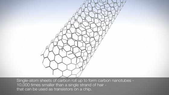
IBM (NYSE:IBM) announced a research breakthrough that could soon permit replacing silicon transistors with carbon nanotubes in future high-performance electronic chips. Carbon nanotubes consist of single atomic sheets of carbon rolled up into a tube. The carbon nanotubes form the core of a transistor device whose superior electrical properties promise several generations of technology scaling beyond the physical limits of silicon.
The IBM researchers developed a fabrication process that permits overcoming previous obstacles in nanotube electronics manufacturing. They demonstrated a new way to shrink transistor contacts without reducing performance of carbon nanotube devices, opening a pathway to dramatically faster, smaller and more powerful computer chips beyond the capabilities of traditional semiconductors. IBM’s breakthrough overcomes a major hurdle that silicon and any semiconductor transistor technologies face when scaling down. In any transistor, two things scale, the channel and its two contacts.
As devices become smaller, increased contact resistance for carbon nanotubes has hindered performance gains until now. These results could overcome contact resistance challenges all the way to the 1.8 nanometer node, four technology generations away. Carbon nanotube chips could greatly improve the capabilities of high performance computers, enabling Big Data to be analyzed faster, increasing the power and battery life of mobile devices, and allowing cloud data centers to deliver services more efficiently and economically. Silicon transistors, tiny switches that carry information on a chip, have been made smaller year after year, but they are approaching a point of physical limitation. With Moore’s Law running out of steam, shrinking the size of the transistor, including the channels and contacts, without compromising performance has been a vexing challenge troubling researchers for decades.
IBM has previously shown that carbon nanotube transistors can operate as excellent switches at channel dimensions of less than ten nanometers, the equivalent to 10,000 times thinner than a strand of human hair and less than half the size of today’s leading silicon technology. IBM’s new contact approach overcomes the other major hurdle in incorporating carbon nanotubes into semiconductor devices, which could result in smaller chips with greater performance and lower power consumption.
IBM has unveiled the first 7 nanometer node silicon test chip, pushing the limits of silicon technologies and ensuring further innovations for IBM Systems and the IT industry. By advancing research of carbon nanotubes to replace traditional silicon devices, IBM is paving the way for a post-silicon future. “These chip innovations are necessary to meet the emerging demands of cloud computing, Internet of Things and Big Data systems,” said Dario Gil, vice president of Science & Technology at IBM Research. “As silicon technology nears its physical limits, new materials, devices and circuit architectures must be ready to deliver the advanced technologies that will be required by the Cognitive Computing era.
This breakthrough shows that computer chips made of carbon nanotubes will be able to power systems of the future sooner than the industry expected.”
For more information please visit: http://www-03.ibm.com