
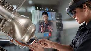
Microsoft HoloLens 2 is a pair of mixed reality smartglasses jointly developed and manufactured by Microsoft and MicroVision, Inc.
HoloLens 2 enterprise edition debuted as the first variant of the device and its followed by a developer edition. The HoloLens 2 are combination waveguide and laser-based stereoscopic & full-color mixed reality smart glasses.
Holographic processing unit (HPU) is Microsoft’s name for the coprocessor in its HoloLens virtual reality (VR) headset.
he HPU conducts the processing that integrates real world and data for augmented reality. All of the integration of environmental data and user input is handled by the HPU.
That FPGA was the precursor to the HPU that the HoloLens headsets now contain. The HPU integrates data from the HoloLens’s sensors (accelerometers to detect motion and a Kinect-like camera system to detect depth). The chip uses those sensors to recognize gestures, maintain a map of the environment, and ensure that virtual 3D objects retain their position in the real world.

The HPU contains 24 Tensilica DSP (digital signal processor) cores. Tensilica DSPs pop up in a few different places; for example, AMD has used them for its TrueAudio audio processing and its hardware-accelerated video codecs. Other companies have built Wi-Fi chips around the Tensilica DSP, too.
The Hogel processing unit (HPU) is a computation for rendering hogels. HPU parallelism Since many (possibly hundreds) HPUs would be required to drive a single light-field display, it is important that the HPU be an independent processor, requiring minimal support logic and interconnect.
The HPU can perform about one trillion floating point operations per second and is 200 times faster than a pure software equivalent. The whole chip draws under 10W, as compared to the 4W used by the Intel Cherry Trail Atom SoC that provides the HoloLens’s CPU and GPU. The HPU provides the CPU with highly processed “cooked” data which is in turn exposed to the 3D programs running on the headset.